
A family of high-performance 64-bit RISC workstations and servers based on the new Digital Alpha AXP architecture is described. The hardware implementation uses the powerful new DECchip 21064 CPU and employs a sophisticated new system interconnect structure to achieve the necessary high bandwidth and low-latency cache, memory, and I/O buses. The memory subsystem of the high-end DEC 3000 AXP Model 500 provides a 512KB secondary cache and up to 1GB of memory. The I/O subsystem of the Model 500 has integral two-dimensional graphics, SCSI, ISDN, and six TURBOchannel expansion slots.
The DEC 3000 AXP system family consists of both workstations and servers that are based on Digital's Alpha AXP architecture. [1] The family includes the desktop (DEC 3000 AXP Model 400) and desk-side and rack-mounted (DEC 3000 AXP Model 500) systems. The available operating systems are the DEC OSF/1 AXP and the OpenVMS AXP systems. All systems use the DECchip 21064 microprocessor. [2]
Table 1 gives the specifications for the three DEC 3000 AXP systems.
| Specifications | Desk-side Model 500 | Rack-mount Model 500 | Desktop Model 400 |
|---|---|---|---|
| Height, inches | 24.7 | 15.75 | 5 |
| Width, inches | 12.75 | 17.5 | 20 |
| Depth, inches | 29.7 | 27 | 16.75 |
| Maximum DC power output, watts | 480 | 480 | 295 |
| Memory Standard, MB | 32 | 32 | 32 |
| Memory Maximum, MB | 1024 | 1024 | 512 |
| Internal hard disc Standard, MB | 1050 | 1050 | 426 |
| Internal hard disc Maximum, MB | 4200 | 4200 | 2100 |
| Serial ports | 2 | 2 | 2 |
| ISDN port | 1 | 1 | 1 |
| SCSI ports (one internal, one external) | 2 | 2 | 2 |
| Ethernet port (AuI (thick wire) and 10Base-T (twisted pair)s | 2 | 2 | 2 |
| TURBOchannel slots | 6 | 6 | 3 |
| Removable media (5.25 inch half-height slots) | 2 | 2 | 1 |
| Integral graphics accelerator | Yes | Yes | No |
| Audio | Yes | Yes | Yes |
The DEC 3000 AXP systems are designed to be significantly faster than all previous Digital workstations and to offer performance competitive with that of other reduced instruction set computer (RISC) workstations currently available. In general, RISC systems have larger code sizes and consequently require more instruction-stream bandwidth than complex instruction set computer (CISC) systems. Further, 64-bit machines require more data-stream bandwidth than 32-bit machines. To complement the power of the DECchip 21064 microprocessor, the systems need a balanced system architecture, including a high-bandwidth, low-latency memory system and an efficient, high-performance I/O subsystem.
Traditional workstation designs that use a common system bus exhibit increased memory latency and reduced memory bandwidth due to system bus contention. This is a special concern for designs using a large number of high-performance I/O devices. Increased latency can also result from the additional levels of buffering and system bus loading common to traditional architectures. Many system buses also exhibit multiplexing between address and data, leading to further performance degradation.
To meet the goals of low memory latency, high memory bandwidth, and minimal CPU-I/O memory contention in a cost-competitive manner, the designers implemented the DEC 3000 AXP system architecture in an unusual way. They chose to build the system interconnect from inexpensive application-specific integrated circuits (ASICs), as shown in Figure 1. The ASICs act as a crossbar between the CPU, memory, and I/0 buses. Addresses and data are switched independently by the crossbar.
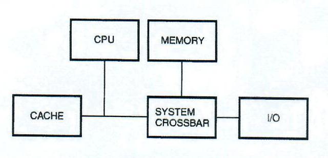
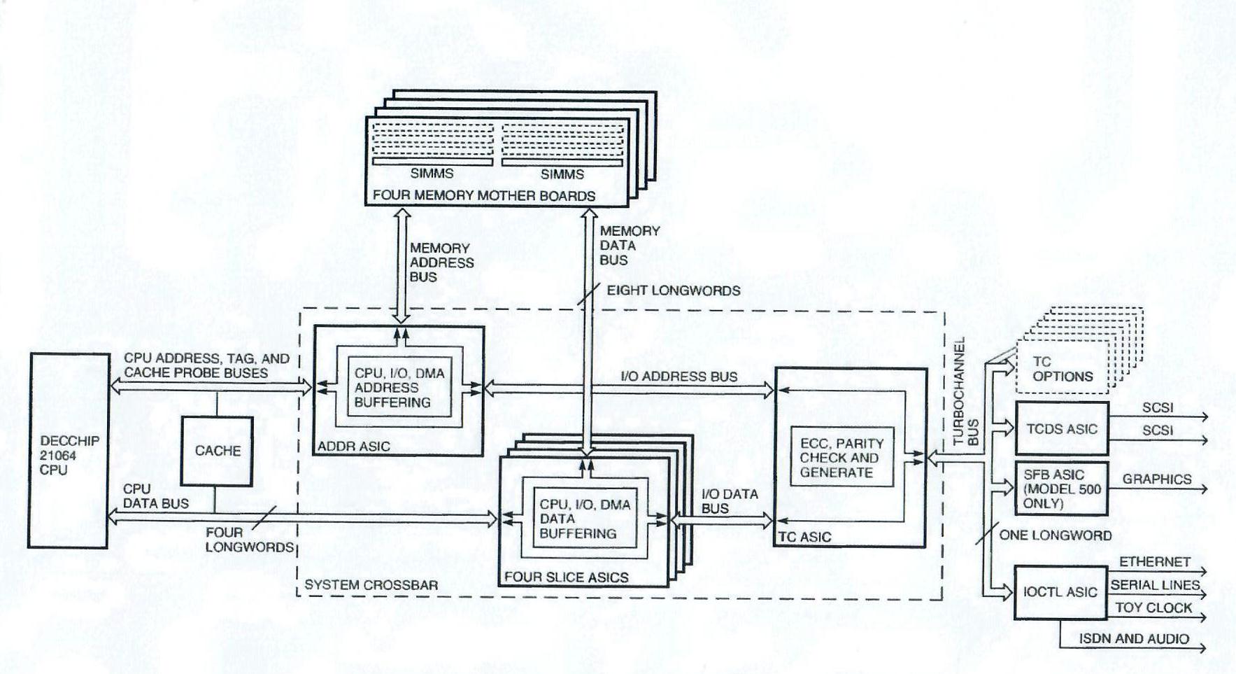
The system block diagram in Figure 2 shows the system architecture of the DEC 3000 AXP systems. The system crossbar in the center of the diagram is composed of six ASICs, consisting of the ADDR ASIC, the TURBOchannel (TC) ASIC, and four SLICE ASICs. The ADDR ASIC switches addresses between the CPU, the memory, and the TC ASIC. The four SLICE ASICs switch data between the CPU, the memory, and the TC ASIC. The TC ASIC switches I/O addresses and data between the ADDR and SLICE ASICs and the TURBOchannel bus. Connected to the TURBOchannel bus are the various I/O controllers, including the dual small computer systems interface (SCSI) controller ASIC, the general I/O controller ASIC, and the two-dimensional graphics accelerator ASIC (not present in DEC 3000 AXP Model 400 systems). In addition, six TURBOchannel option slots are available for expansion (three slots in DEC 3000 AXP Model 400 systems).
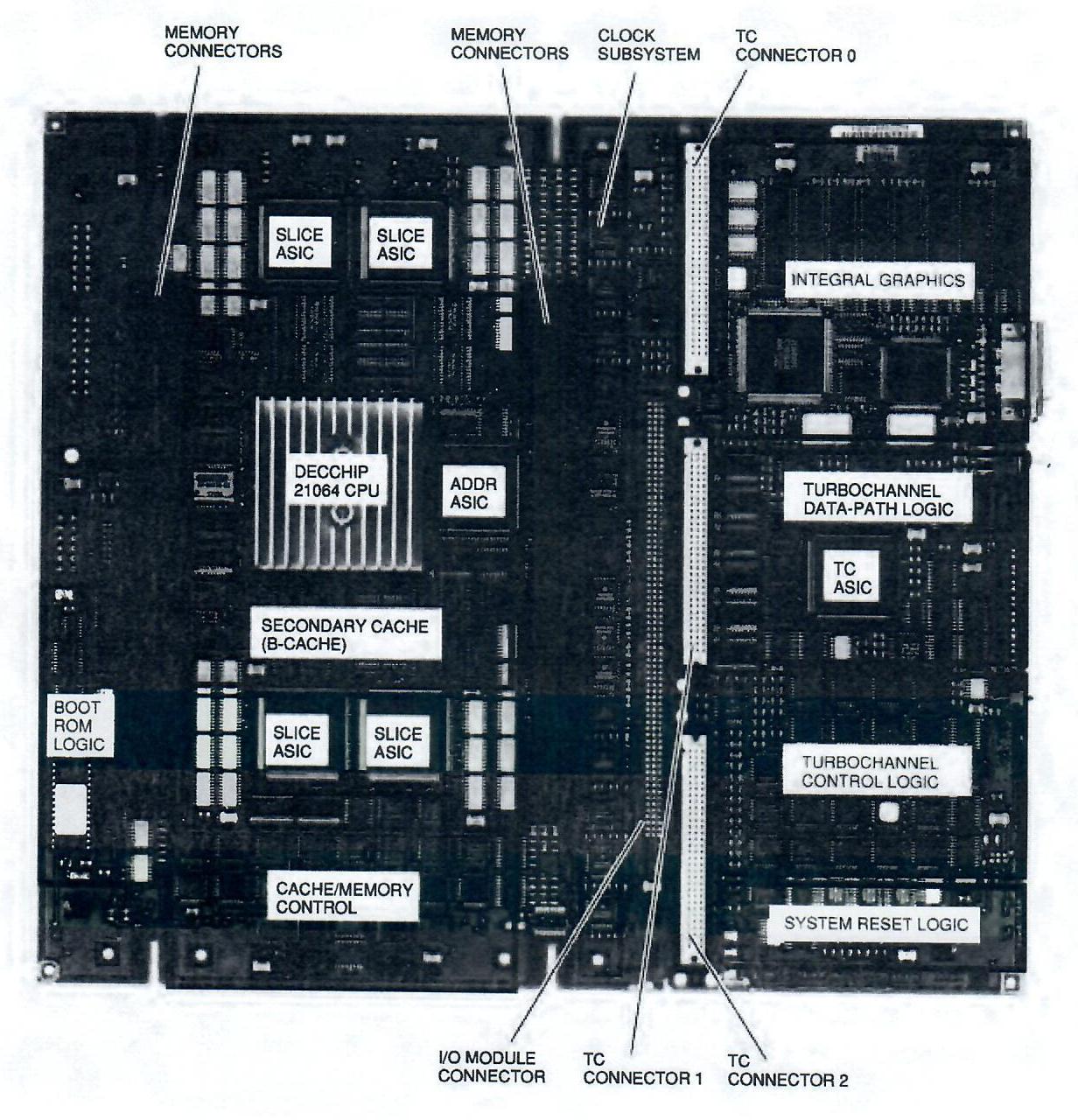
The DEC 3000 AXP systems are composed of two primary modules, the CPU module and the I/O module. The CPU module contains the processor, secondary cache, control logic, TURBOchannel interface and, in the Model 500, the two-dimensional graphics subsystem. It has connectors for the I/O module, four memory mother boards, a lights and switches module (LSM), three TURBOchannel options, and the power supply. Figure 3 shows the layout of the module.
The DECchip 21064 microprocessor is the CPU of the DEC 3000 AXP systems. On the Model 500, the CPU runs at 150 megahertz (MHz), and on the Model 400, it runs at 133 MHz. The processor is a superscalar, fully pipelined implementation of the Alpha AXP architecture. [2] It contains two on-chip 8-kilobyte (KB) direct-mapped caches, one for use as an instruction cache, the other as a data cache. Both the integer and floating-point units are contained on-chip.
The system employs a second-level cache (B-cache) to help minimize the performance penalty of misses and write throughs in the two relatively small 8KB primary caches of the DECchip 21064 processor. The B-cache is a 512KB, direct-mapped, write-back cache. A direct-mapped cache eliminates the logic needed to choose among the multiple sets of a set-associative cache, resulting in a faster cache cycle time. A write-back protocol was selected because it reduces the amount of write traffic from the B-cache to main memory, leaving more main memory bandwidth available for other memory transactions.
The block size of the B-cache is 32 bytes, matching the block size of the primary caches. The cache block allocation policy used is to allocate on both read miss and write miss. Hardware keeps the cache coherent on direct memory access (OMA) transactions; DMA reads probe the cache and DMA writes update the B-cache (and invalidate the primary data cache).
The DEC 3000 AXP systems are designed to be uniprocessor systems, which simplifies the cache controller design in a number of ways. For example, since no other CPU's cache can contain a copy of a cache block, there is no need to implement cache coherency constructs such as a shared bit. Further, by loading the B-cache during the power-up sequence and keeping it coherent during DMA by using an always-update protocol, cache blocks in the B-cache are always guaranteed to be valid. This method eliminates stale data problems without needing to use a valid bit.
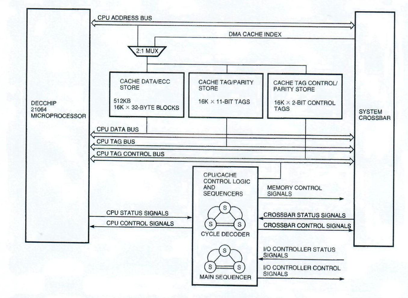
In addition to the cache memory, the subsystem consists of the cache controller, the main memory controller, and the protocol control logic for memory access arbitration. A block diagram of the CPU and B-cache subsystem is shown in Figure 4.
The B-cache is alternately controlled by the CPU and the external cache controller. When controlled by the CPU, the cache may be read by the CPU in five CPU cycles. The cache data bus width is 16 bytes, therefore two reads are necessary to fill a cache block. The Model 500 has a maximum cache read bandwidth of 480 megabytes per second (MB/s). The cache may be written by the CPU with an initial tag probe latency of five CPU cycles followed by up to two write cycles of five CPU cycles each. The Model 500 has a cache write bandwidth of 320 MB/s.
When a CPU probe misses in the B-cache, or when the CPU accesses the external lock register, control of the cache is turned over to the external cache controller. This logic controls filling the cache with the required data from main memory, handing the data to the CPU during reads, merging CPU write data into the cache on writes, and maintaining the contents of the external cache tag and tag control store. In addition, this logic maintains the architecturally defined lock flag and locked physical address register, which can be used to implement software semaphores and other constructs normally requiring atomic read-modify-write memory transactions.
The control logic for the B-cache consists of two interlocking state machines. These state machines control arbitration and decoding of processor and I/O subsystem requests. They also generate the control signals needed to execute these requests to the CPU, B-cache, and main memory.
The state machines prioritize and arbitrate requests from various sources, including the CPU, the I/O subsystem, and the memory refresh logic. Arbitration is done according to a fixed priority. First priority goes to DMA requests from the I/0 subsystem. Second priority goes to memory refresh requests. Lowest in priority are requests made by the CPU. The one exception to this scheme occurs at the conclusion of a DMA transaction. In this case, the first arbitration cycle following the DMA changes the priority to memory refresh first, CPU request second, and DMA last. This guarantees that requests for CPU and memory refreshes are granted during heavy DMA traffic.
The larger state machine, or main sequencer, examines the command generated by the smaller state machine, or cycle decoder, and initiates the control flow necessary to perform that command. Fifteen unique flows are implemented by the main sequencer. They are
When a cache miss occurs and the new cache block replaces a cache block that has been modified, as indicated by the "dirty" status bit, the displaced data is referred to as a "victim block" or "victim data."
The many variants of cacheable reads and writes provide optimized flows that maximize the parallelism of cache accesses and memory accesses. For example, during the "read cacheable memory with victim block" flow, the main sequencer reads the victim block from the B-cache and stores it in the SLICE ASICs in parallel with reading the new block from main memory. The same flow without a victim block makes use of the main memory access time to update the tag store. The control flows for writes to cacheable memory also take advantage of this parallelism. A further write optimization is used when the cycle decoder determines that the entire cache block will be written; in this case the data from memory is completely overwritten, and therefore it is never fetched from memory.
DMA flows are entered upon request of the DMA controller in the I/O control section. DMA control flows start by asserting a "hold request" to the CPU, causing the CPU to cease B-cache operations within a specified time, after which it asserts a "hold acknowledge" signal. It should be noted that the CPU will continue to execute instructions internally until such time as it experiences a miss in one of its internal caches, or it requires some other external cycle.
Each DMA write to memory results in a probe of the B-cache for the DMA target block, with a hit resulting in the B-cache block being updated in parallel with main memory and the corresponding primary data cache block being invalidated. DMA reads cause main memory to be read in parallel with probes and reads of the B-cache. If a cache probe hits, the B-cache data is used to fill the DMA read buffer in the SLICE ASICs; otherwise the main memory data is used. In this manner, cache coherence is maintained.
The DEC 3000 AXP Model 400 and Model 500 architecture supplants the traditional system bus with a system crossbar constructed from ASICs. Tightly coupled to the crossbar is the system memory. Three types of ASICs - SLICE, ADDR, and TC - form the crossbar. SLICE and ADDR are discussed next and TC is discussed in the I/O Subsystem Interface section.
The four SLICE ASICs are used strictly for data path; together they form a 32-byte bus to main memory, a 16-byte bus to the CPU and cache, and a 4-byte bus to the TC ASIC. It is helpful to think of the SLICE ASICs as a train station for data with the data buses as train tracks. Data can come and go on any track, different tracks have different speeds and widths, and data can find temporary storage in the ASICs. The SLICE ASICs provide the systems with a location to buffer DMA, I/O read, I/O write, and victim data while the data waits to travel the next leg of its journey. The use of the SLICE ASICs also eliminates one to two levels of buffering between the dynamic random-access memories (DRAMs) and the CPU, thus decreasing latency and improving bandwidth.
A key design decision was determining the width of the memory data bus. A conventional design would have matched the width of the memory bus to the width of the cache bus (16 bytes). However, to reduce the memory latency of the second half of the cache block (cache line size is 32 bytes), the system reads the entire cache block from memory at once using a 32-byte memory bus. This technique eliminates the additional latency from a second page-mode read.
The DEC 3000 AXP Model 500 returns the entire block to the cache and CPU with an average latency of only 180 nanoseconds (ns) from the CPU memory request. In contrast, a less aggressive preliminary design using a system bus and 16-byte-wide memory bus yielded an average memory latency of 320 ns. The 32-byte memory bus costs little more than a 16-byte bus-two low-cost ASICs, resistor packs, and some address fan-out parts.
The ADDR ASIC is a crossbar for addresses. ADDR sends addresses from the CPU to memory (CPU reads and writes), from the CPU to I/O (I/O reads and writes), and from the I/O to CPU and memory (DMA reads and writes). ADDR selects between CPU read, victim write, and DMA addresses to send to memory. A counter that increments DMA addresses on long TURBOchannel DMAs also resides in ADDR.
ADDR provides a home to the memory configuration registers. At power-on time, the boot firmware writes and reads memory space, determines the memory configuration, and writes the configuration registers. At run time, each memory address maps into a unique bank, regardless of the type and order of the single in-line memory modules (SIMMs) installed.
ADDR also provides a home for miscellaneous functions such as tag parity checking, refresh counter, and the locked physical address register. It generates the cache probe index to check the cache tags for a hit or a miss on DMA probes.
The memory system is composed of memory mother boards (MMBs) that rise from the system card, and SIMMs. This arrangement is a good solution to the problem of limited space on the system module. It allows for a wide data bus and for good signal integrity for short propagation times on the memory data bus.
As shown in Figure 5, an MMB module supports up to eight SIMMs at a time (four SIMMs in Model 400 systems). A minimum of two SIMMs is required for each board. A system always contains four MMBs. The MMBs act as a carrier for the SIMMs and also contain drivers for address and control signals.
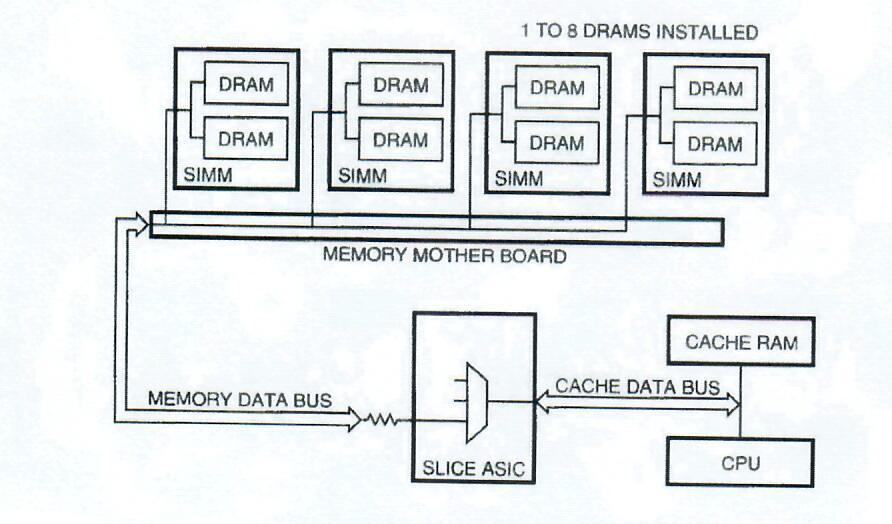
A total of 8, 16, 24, or 32 SIMMs (maximum of 16 in Model 400 systems) can be plugged into the system. SIMMs may be single- or double-sided with 10 DRAMs per side. Each side of a SIMM constitutes one eighth of a bank. Eight SIMMs must be plugged in to complete a bank; hence the 320-bit-wide data bus (4 bits per DRAM by 10 DRAMS per SIMM by 8 SIMMS). One megabit (Mb), 4Mb, and 16Mb DRAMs are supported, and users are allowed to populate banks in any order. In this way, the DEC 3000 AXP Model 500 can support from 8MB to 1 gigabyte (GB) of memory, and the DEC 3000 AXP Model 400 can support 8MB to 512MB of memory.
Main memory is protected by a single-bit-correct, double-bit-detect error-correcting code (ECC). In addition, the arrangement of data bits allows the detection of any number of errors restricted to a single DRAM chip. ECC corrections for CPU transactions are performed by the CPU, and corrections for I/O transactions are done in the TC ASIC.
When data is stored in the B-cache by the CPU, it is not immediately sent to memory. Data is written to main memory only when a dirty block in the cache is replaced. Data destined for the cache is read from main memory only on cache misses. Reads to main memory, whether from the CPU or from DMA, always return 32 bytes. On CPU reads of main memory, data is returned to the cache and CPU in two halves by the SLICE ASICs. Likewise when the B-cache control writes victim data to main memory, two reads are made of the cache, but only one write is made to main memory.
On DMA writes, 4 bytes of data arrive from the TURBOchannel interface ASIC each cycle and are stored in the SLICE ASICs. The SLICE ASICs can buffer up to 128 bytes of data prior to writing the data to main memory using page-mode writes, 32 bytes at a time. To maintain cache/memory coherence, data is also provided to the cache RAMs so that it may be written in the case of a cache hit. On DMA reads, up to 128 bytes of data are read page mode out of main memory and buffered in the SLICE ASICs. Data flows out to the TC ASIC and the TURBOchannel bus at the rate of 4 bytes per cycle (100MB/s). In the event of a cache hit, data is taken preferentially from the cache.
The crossbar employs a technique that permits simultaneous transactions from CPU to main memory and DMA. The TURBOchannel bus supports DMA transactions of up to 512 bytes in length. Once the DMA starts, the system must be able to provide or receive data without any gaps. However, while the DMA buffer in the SLICE ASICs is sufficiently full (for DMA reads) or empty (for DMA writes), the CPU is allowed to use memory. When the I/O controller detects that the buffer is too full or too empty, it requests memory time to service the DMA buffer. At this time, further CPU requests are temporarily ignored. This technique prevents the CPU from being locked out of main memory, even during long DMA transactions and even though DMA has priority over CPU transactions.
The crossbar also permits simultaneous write transactions from the CPU to main memory and from the CPU to an I/O device. SLICE and ADDR ASICs can buffer one I/O write transaction of up to 32 bytes in size. Once the ASICs have accepted the data and address, the cache and crossbar are free to process other CPU transactions, which can include cache and main memory reads and writes. If the CPU issues an I/O write while a previous write is still pending in the ASICs, the cache controller simply stalls.
The I/O system is based on the TURBOchannel, a 32-bit high-performance, bidirectional, multiplexed address and data bus developed by Digital for workstations. [3] The DEC 3000 AXP supports up to six plug-in options, as well as the integral smart frame buffer (SFB) graphics ASIC, the I/O controller (IOCTL) ASIC, and the TURBOchannel dual SCSI (TCDS) ASIC. The TURBOchannel bus is synchronous and requires only five control signals in each direction between the system and the option cards.
The system interfaces to the TURBOchannel bus by a data-path TC ASIC and control logic contained in a number of programmable array logic devices (PALs). The TC ASIC completes the system crossbar by passing addresses between the TURBOchannel bus and the address ASIC, and passing data between the TURBOchannel bus and the SLICE ASICs. Furthermore, the TC ASIC checks and generates parity on the TURBOchannel, and checks, corrects, and generates ECC on the data bus to the SLICE ASICs. Parity checking of TURBOchannel data is optional and is enabled on a per-option basis through a configuration register in the TC ASIC. Finally, the TC ASIC contains a number of counters for tracking DMA progress, as well as configuration and error registers. All control logic was implemented in PALs to minimize the impact to the project schedule of any design changes. The TURBOchannel interface block diagram in shown in Figure 6.
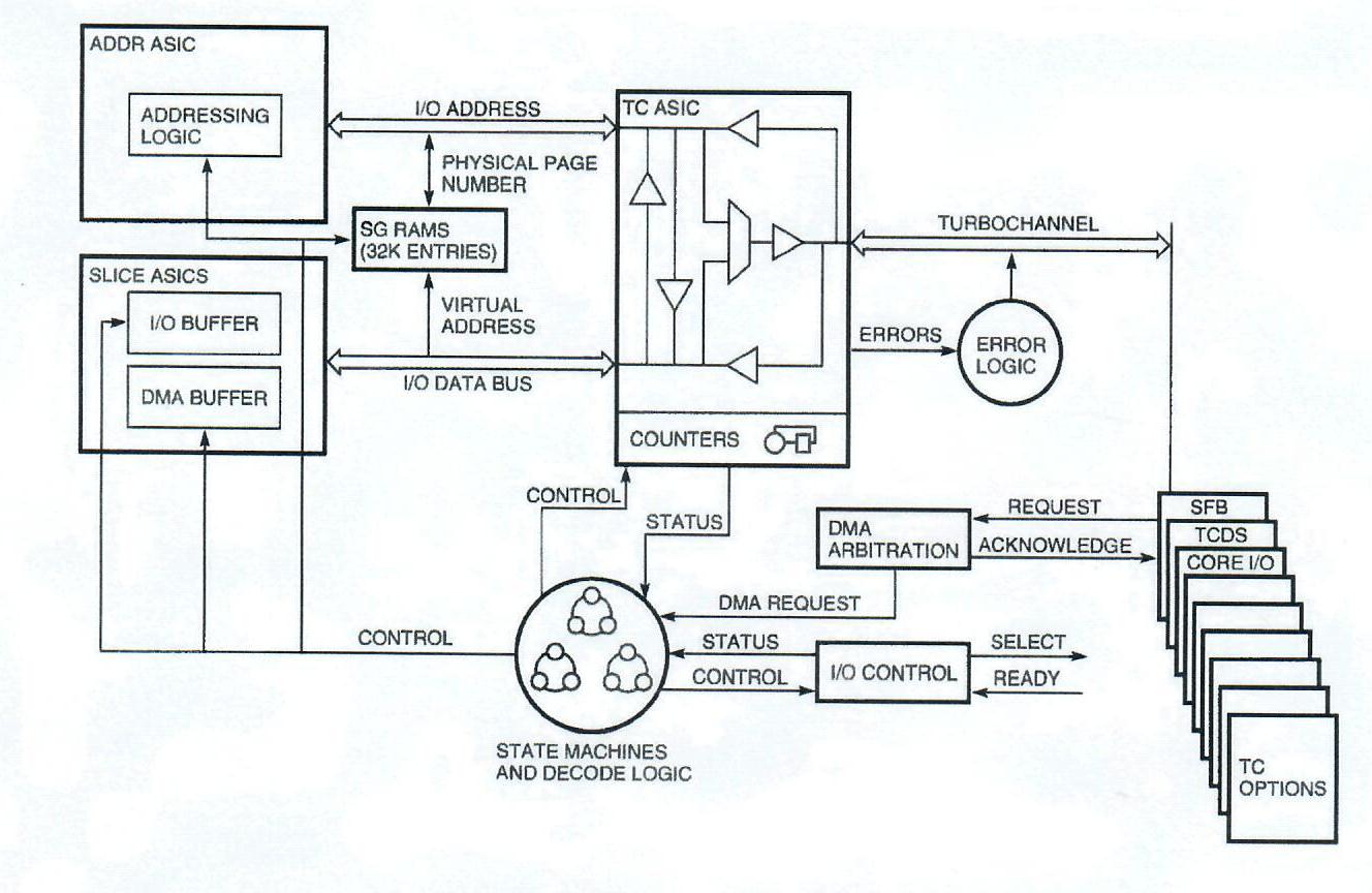
There are two types of TURBOchannel operations: the system initiates I/O reads and writes, and the options initiate DMA reads and writes. On an I/O operation, the system sends the I/O address from the ADDR ASIC to the TC ASIC, and from there to the TURBOchannel. For I/0 reads, the option returns data on the TURBOchannel. This data passes through the TC ASIC and over the bus to the SLICE ASICs. The system includes some special hardware for byte masking of I/O read data. This hardware is used to provide support for VMEbus adapters.
For I/O writes, the system sends data from the SLICE ASICs across the data bus to the TC ASIC. The TC ASIC then sends it to the option over the TURBOchannel. The DEC 3000 AXP workstation supports a block write extension to the original TURBOchannel protocol. In this mode, the system supplies a single address followed by multiple consecutive data transfers for improved I/O write performance. This extension is also configurable on a per-option basis through the TC configuration register.
The TURBOchannel protocol specifies that before any option can use the bus for DMA, it must issue a request to the system. The DEC 3000 AXP architecture employs an arbitration scheme using rotating priority that prevents any option from being locked out. After being granted the bus, the option supplies a DMA address on the TURBOchannel bus. This address routes through the TC ASIC and onto the address ASIC. In the case of a DMA write, data immediately follows the address on the TURBOchannel. This data passes through the TC ASIC and onto the data bus to the SLICE buffers.
DMA reads are more complicated than writes because the TURBOchannel bus does not transmit ahead of time the number of bytes of data to be read from memory. Instead, it continues to assert its read request signal for as long as it is requesting data. The SLICE buffers begin to fill up with DMA data, and only when they can guarantee that there will be no gaps in the DMA will the data transfer start. The TC ASIC receives the read data from the SLICE ASICs and sends it onto the TURBOchannel to the requesting option.
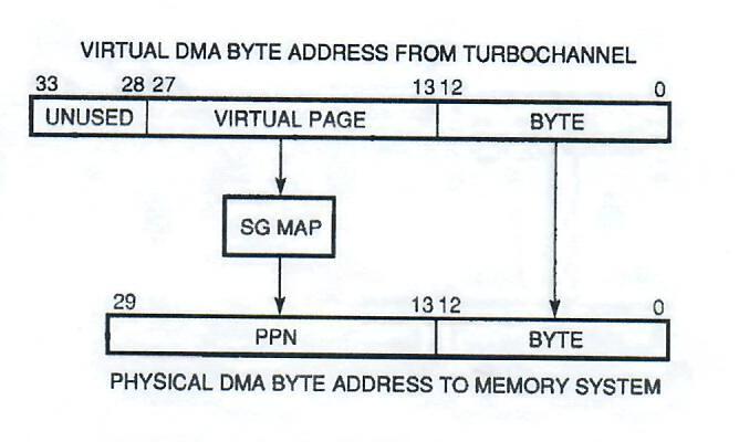
Virtual DMA allows the system to map non-contiguous regions of physical address space into contiguous regions of virtual address space. This method allows TURBOchannel options to transfer large blocks of DMA data without knowledge of how that data is mapped in the physical address space in main memory. Virtual DMA enhances operating system performance because the memory mapping is performed before the transfer of DMA data.
The DEC 3000 AXP workstation supports virtual DMA through the use of a scatter/gather (SG) map, which acts as a translation buffer. SG mapping is enabled on a per-option basis through the configuration register in the TC ASIC. The SG map is organized as 32K 24-bit entries. Each entry contains a 17-bit physical page number (PPN), parity, and valid bit. Software sets up the map through I/O space reads and writes. DMA byte address bits [27:13] index the SG map, which produces a 17-bit PPN (bits [29:13]) to append to the virtual DMA byte address bits [12:0]. The resulting 30-bit physical DMA byte address can then address all 1GB of the possible system address space. An S/G map is shown in Figure 7.
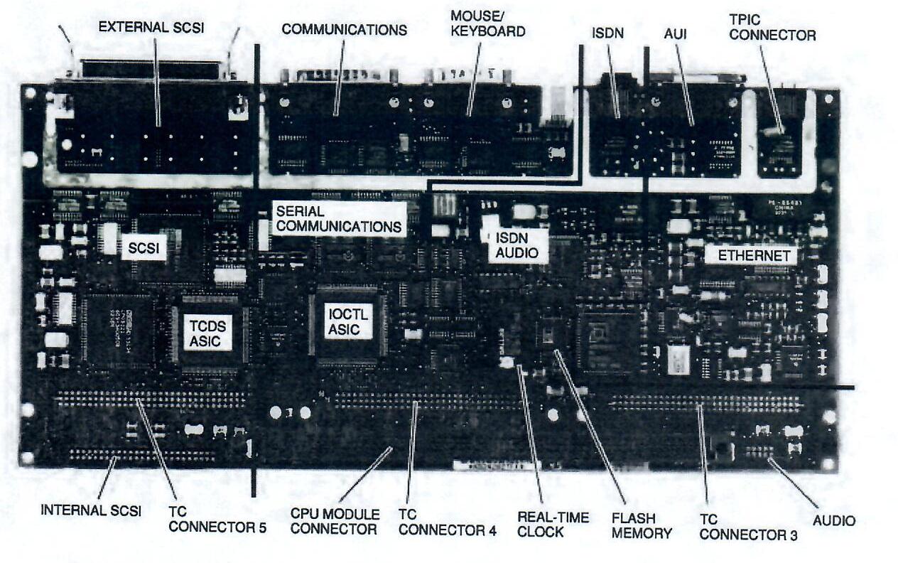
Most of the I/O subsystem is implemented on its own module. This I/O module, shown in Figure 8, contains the connectors for attachment unit interface (AUI) Ethernet, l0Base-T Ethernet, Integrated Services Digital Network (ISDN), alternate console/serial printer, mouse/keyboard, communications, internal and external SCSI, three TURBOchannel options, and audio module port. The various I/O controllers interface to the TURBOchannel through one of three ASICs. These ASICs are the smart frame buffer (SFB) on the CPU module and the TURBOchannel dual SCSI (TCDS) ASIC and the I/O controller (IOCTL) ASIC on the I/O module.
A key I/O subsystem design decision was to reduce time-to-market by eliminating unnecessary new hardware and software development. To support most of the I/O functionality, the designers chose the IOCTL ASIC developed for the DECstation 5000 Model 240.
The IOCTL ASIC provides an interface to a 16-bit, general-purpose I/O bus, which supports the following devices: two Zilog Z85C30 serial communications controllers (SCCs), an AMD 7990 local area network controller for Ethernet (LANCE), a Dallas semiconductor DS1287 real-time clock, an AMD 79C30A ISDN data controller (IDC), a SCSI controller, and an AMD 27C020 256KB erasable programmable read-only memory (EPROM).
The SCCs implement the keyboard, mouse, alternate console/printer, and communications ports. The mouse and keyboard do not use DMA. The alternate console/printer and the communications port do use DMA.
The LANCE implements the Ethernet interface, which connects to the local area network (LAN) through either the AUI (thickwire) or l0Base-T (twistedpair interconnect [TPIC]) connectors. Software controls which one of these interfaces is enabled.
The real-time clock provides time-of-year (TOY) reference and 50 bytes of nonvolatile RAM. A lithium battery supplies power in the event of system power-off or failure.
The IDC implements both an ISDN interface and telephone-quality audio. The audio connects to the audio interface module (AIM), which provides the audio I/O in the Model 500. Audio I/O in the Model 400 is on its I/O module.
The AIM on the Model 500 supports audio input through either a 1/8-inch minijack for microphone input, a 4-pin modular jack (MJ) connector for use of a telephone handset, or an RCA-style phonograph jack used as a line-in input. Output is provided by the MJ connector as well as by a 1/8- inch stereophonic jack. The stereophonic jack accepts only a stereophonic plug. If monophonic headphones are used, a mono-to-stereophonic adapter is required. On the Model 400, audio input and output is implemented using a 4-pin MJ connector.
Analysis of the complete audio system in a Model 500 shows a frequency response of 145 Hz to 3,500 Hz, with typical distortion in the 0.8 percent to 1.9 percent range for the microphone and 0.4 percent to 1.5 percent for the telephone handset. The signal-to-noise ratio ranged
Although the IOCTL ASIC contains an interface to a SCSI controller, the DEC 3000 AXP systems implement their SCSI interface using the TCDS ASIC. This design has several advantages. First, the TCDS ASIC supports two SCSI ports rather than the one supported by the IOCTL ASIC, permitting separate internal and external SCSI chains. Second, this design eliminates contention between the Ethernet controller and the SCSI controller for the IOCTL bus. Third, the TCDS ASIC supports much longer TURBOchannel DMA bursts (64-byte bursts rather than 16-byte bursts). Finally, the resulting ASIC design is used to implement a dual SCSI TURBOchannel option module.
The TCDS ASIC implements two separate SCSI ports using two NCR 53C94 advanced SCSI controllers (ASCs). The TCDS allows both controllers to have DMA transfers in progress simultaneously.
TCDS TURBOchannel DMA transactions are aligned 64-byte blocks. Starting DMA addresses that are not aligned to these boundaries begin with a smaller DMA transaction. This technique aligns the address so that succeeding transactions are aligned 64-byte blocks. Large, aligned transactions increase both TURBOchannel and memory access efficiency.
The TCDS ASIC and the ASCs provide odd parity protection on major data paths. This protection includes 8-bit parity on the 16-bit bus between the TCDS and the ASCs, 32-bit parity on TCDS DMA buffer entries, and 32-bit parity on TURBOchannel transactions, both I/O and DMA.
The graphics subsystem on the Model 500 system card provides integral 8-plane graphics with hardware enhancements for improved frame buffer performance. These enhancements increase the performance of stipple, line drawing, and copy operations. The graphics system consists of an SFB ASIC, 2MB video RAM, and the Brooktree Bt459 RAMDAC chip for sourcing the Splane RGB data. The user can select either a 66-Hz or a 72-Hz monitor refresh rate through a switch on the back of the workstation. The graphics subsystem can draw 615K two-dimensional vectors per second and can perform copy operations at 31.8MB/s.
The graphics subsystem is available separately as the TURBOchannel HX graphics option card. In addition, high-performance two-dimensional and three-dimensional graphics accelerators are available through the TURBOchannel bus for all systems.
The input clock circuitry to the DECchip 21064 CPU contains a differential 300-MHz oscillator (266 MHz for the Model 400), which drives an alternating current (AC) decoupling circuit and the CPU chip. The CPU chip divides down the input clock frequency by a factor of two and operates internally at 150 MHz. The DEC 3000 AXP Model 500 is capable of supporting a 200-MHz CPU with a 400-MHz oscillator.
The entire system, with the exception of some I/O devices, runs synchronously. The master system clock is generated by the CPU chip at a frequency of 25 MHz (22 MHz for the Model 400), resulting in system clock cycles of 40-ns duration. This master system clock is duplicated and distributed with differential pseudo-emitter coupled logic (PECL) to maintain minimum skew and to improve noise margin. The PECL clocks are converted to transistor-transistor logic (TTL) in the last stage of the clock fan-out tree.
Two stages of system clock fan-out are used as shown in Figure 9. Two MCl00Elll ECL clock buffer chips (PECL input and output) provide 18 low-skew differential copies of the clock. Seventeen MC100H641 ECL-to-TTL converters (PECL input, TTL output) are distributed throughout the system and I/O boards to provide more than 100 clock lines. All clock lines are length matched to reduce skew, and PECL wires are separated from TTL. Worst-case SPICE simulation indicates a skew between typical components such as PALs to be 1.5 ns. Actual skews measured in the lab are approximately 0.5 ns.
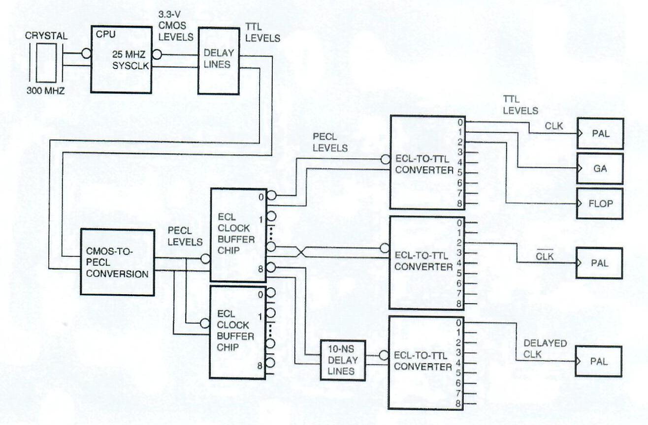
To give designers maximum flexibility, four phases of the system clock are generated, one every 10 ns. Delay lines are used to generate an offset of 10 ns. By swapping the high and low differential inputs to selected MC100H641 converters, the 20- and 30-ns delayed clocks are generated. The master system clock is delayed using delay lines so that the eventual system clock is synchronous with the CPU chip.
The nine ASICs in a DEC 3000 AXP workstation use six unique 1.0-micrometer complementary metal-oxide semiconductor (CMOS) designs. (See Table 2.) Plastic quad flat packs (PQFP) are used as the packaging technology to limit device cost. Because the ASICs are I/O limited and the PQFPs do not have ground planes, the effects of simultaneous switching outputs (SSOs) were a concern. The potential effects of SSOs in CMOS output buffers include corrupted data and undesirable oscillations. Simulation and bench characterization were used to quantify the SSO effects, and in some cases SSOs were reduced by staggering output driver timing.
| Chip | Total nu,ber of pins | Number of pins used | Number of Signal Pins | Used Gates | Available Gates |
|---|---|---|---|---|---|
| SFB | 184 | 184 | 150 | 21.6K | 54K |
| TC | 184 | 182 | 144 | 12.1K | 44K |
| SLICE | 184 | 184 | 153 | 11.2K | 44K |
| ADDR | 184 | 183 | 148 | 5.7K | 44K |
| TCDS | 120 | 120 | 94 | 26.5K | 68K |
| IOCTL | 160 | 160 | 126 | 11.2K | 44K |
Although ASICs were chosen for the data path, PALs were used for control logic due to their greater flexibility and faster turnaround time. A total of 63 20XX (5 ns) and 22V10 (10 ns) PALs with 57 different codes was used. Exhaustive system-level simulation and bench characterizations were performed to understand device behavior in the many different loading scenarios.
The CPU board technology proved moderately difficult for system-level assembly due to the large distance between the fine-pitch (25 mil) components. There are 19 fine-pitch components on the 14- by 16-inch CPU board, with a maximum distance of 14 inches between any two devices. With this large distance, an aggressive, true positional diameter (TPD) tolerance requirement of 6 mils was implemented. TPD is defined as the total diameter of permissable movement from a theoretical exact location around the true position of the pads. This TPD requirement ensures proper positional accuracy between the solder paste stencil apertures and the surface-mount features. In addition, solder mask between pads on the fine-pitch components is used to reduce manufacturing defects.
To reduce power and cost, the slower DEC 3000 AXP Model 400 design substitutes CMOS technology for the BiCMOS cache SRAMs and for many of the bipolar PALs.
The following fixed disk drive options are currently available.
The following removable media options are also available.
The Model 500 has a 480-watt output, off-line, switching regulated power supply, which includes a capacitor-input, automatic voltage-selecting circuit to permit worldwide operation without a voltage-select jumper for 120 or 240 volt (V) input. The power supply provides five outputs to the load: +3.3 V, +5.1 V-CPU, +5.1 V-turbo, +12.1 V, and -12.1 V.
The power supply also provides power for three external fans. Temperature-sensing fan speed control is provided to reduce system noise. The power supply senses tachometer outputs from the fans, and when a fan fails, it shuts down and illuminates an indicator.
The designers provided several debugging features, including test points on the module, tristate outputs on ASICs and PALs, an on-board diagnostic ROM, and programmable console ROM. Since the module is composed almost exclusively of surface-mount devices, the designers specified as many vias as possible for use as test points. Consequently, all wires on the board have test points, which allows for 100 percent short-circuit coverage and 94 percent open-circuit coverage.
The DEC 3000 AXP workstation takes full advantage of the serial ROM port on the DECchip 21064 CPU. This port allows code to be directly loaded into the instruction cache. During prototype development, designers loaded special debug programs into the CPU through this port. However, the real innovation is in also wiring this port to the output of a 64K by 8 EPROM on the module to provide 8 programs that are individually selectable by moving a jumper on the module. On system reset, serial program data from the selected EPROM output is loaded into the instruction cache. These programs include powerup code for loading the real console, a miniconsole, and five diagnostic programs for testing memory and the graphics subsystem. Other tests are available by replacing the EPROM. These programs are of great value in the manufacturing debug environment.
Two flash EPROMs contain the console code for the system. On power-up, code in the serial ROM loads the console code into memory and begins executing it. Users can easily update the console ROMs (for example, to provide PAL code enhancements) through a special utility booted off a CD-ROM connected to the system. Field service can update the console code in the system remotely through the Ethernet.
The primary goal of this project was to design a balanced system that exhibited low memory latency, high memory bandwidth, and minimal CPU-I/O memory contention in a cost-effective manner. Table 3 gives the measured performance numbers for these characteristics. Except where noted, all numbers are for sustained performance. Of particular note are the numbers showing that the CPU receives significant memory bandwidth even in the presence of heavy block I/0 and DMA traffic.
| DEC 3000 AXP Model 500 | DEC 3000 AXP Model 400 | |
|---|---|---|
| CPU speed | 150MHz | 133MHz |
| B-cache size | 512KB | 512KB |
| B-cache read bandwidth | 480MB/s | 426MB/s |
| B-cache write bandwidth | 320MB/s | 284 MB/s |
| Maximum main memory | 1GB | 512MB |
| CPU memory latency (average) | 32bytes/180ns | 32bytes/203ns |
| CPU memory read bandwidth | 114MB/s | 101MB/s |
| CPU read with victim write memory bandwidth | 160MB/s | 141MB/s |
| TURBOchannel peak bandwidth | 100MB/s | 89MB/s |
| I/O read bandwidth 8 bytes | 13MB/s | 12MB/s |
| I/O write bandwidth 8 bytes | 33MB/s | 29MB/s |
| Block I/O write bandwidth 32 bytes | 67MB/s | 59MB/s |
| Block I/O write bandwidth 32 bytes with CPU read and victim write memory bandwidth | I/O=53MB/s MEM=107MB/s | I/O=47MB/s MEM=95MB/s |
| DMA read bandwidth 512 bytes | 91MB/s | 81MB/s |
| DMA read bandwidth 64 bytes | 57MB/s | 51MB/s |
| DMA write bandwidth 512 bytes | 93MB/s | 82MB/s |
| DMA write bandwidth 64 bytes | 59MB/s | 52MB/s |
| 64-byte DMA write bandwidth with CPU reads from memory | DMA=59MB/s CPU=30MB/s | DMA=52MB/s CPU=27MB/s |
Another goal of the project was to offer performance that is competitive with RISC workstations available from other vendors. The benchmark performance of any system derives from the interdependent performance of the hardware, the operating system, and the compilers that generate the application code. The benchmark performance should improve as each element matures. Table 4 shows the performance of the DEC 3000 AXP systems on a selected set of benchmarks as of the announcement dates of these products. Table 5 compares the performance of the DEC 3000 AXP Model 500 to the published performance of several currently available competitive systems. [4]
| DEC 3000 AXP Model 500 | DEC 3000 AXP Model 400 | |
|---|---|---|
| Clock (MHz) | 133 | 150 |
| SPECmark89 | 108.1 | 121.5 |
| V1.1 (Dhrystones per second) | 228.3K | 257.7K |
| V2.1 (Dhrystones per second) | 249.6K | 281.2K |
| LINPACK 64-bit double precision 100×100 (MFLOPS) | 26.4 | 30.2 |
| LINPACK 64-bit double precision 1000×1000 (MFLOPS) | 70.8 | 79.9 |
| X11PERF Two-dimensional vectors per sec | 564.0K | 636.0K |
| X11PERF Two-dimensional pixels per sec | 27.4M | 31.0M |
| DEC 3000 Model 500 | IBM RS6000 Model 580 | HP9000 Model 750 | |
|---|---|---|---|
| SPECmark89 | 121.5 | 126.2 | 86.6 |
| V1.1 (Dhrystones per second) | 257.7K | n/a | 133.7K |
| V2.1 (Dhrystones per second) | 281.2K | n/a | 122.3K |
| LINPACK 64-bit double precision 100×100 (MFLOPS) | 26.4 | 38.1 | 23.7 |
| LINPACK 64-bit double precision 1000×1000 (MFLOPS) | 79.9 | 84.0 | n/a |
The DEC 3000 AXP Model 500 design was a team effort-more people were involved than can be acknowledged in this space. Recognition is due to those who contributed to the design of original hardware: Dave Archer, Mark Baxter, John DeRosa, Chris Gianos, Leon Hesch, Dave Laurello, Bob McNamara, Dick Miller, Rick Rudman, Dave Senerchia, Petr Spacek, Bob Stewart, Ned Utzig, Debbie Vogt, and John Zurawski. The tight schedule could not have been met without the special efforts of the Power and Packaging, Console, Qualification, Proto Management, and Technology and Operating Systems Groups. The design team for the DEC 3000 AXP Model 400 project is also recognized: John Day, Jamie Pierce, Dennis Rainville, and Ken Ward. The thorough device evaluations by Rob Zahora contributed significantly to the success of the projects. We would also like to acknowledge the contributions by FXO personnel. The Electronic Storage Development Group was responsible for the design of the DEC 3000 AXP Model 500 memory module. Significant efforts by the Maynard TME, Albuquerque, and Ayr Manufacturing Plants should be recognized for delivering quality hardware during the development and production phases; a special thanks to Jim Ersfeld for his significant efforts in this regard.
1. R. Sites, ed., Alpha Architecture Reference Manual (Burlington, MA: Digital Press, Order No. EY-L520E-DP, 1992).
2. D. Dobberpuhl et al., A 200-MHz 64-bit Dual-issue CMOS Microprocessor, IEEE Journal of Solid-State Circuits, vol. 27, no. 11 (November 1992) 1555-1567 and Digital Technical Journal, vol. 4, no. 4 (1992, this issue).
3. TURBOchannel Specifications, Version 2C (Palo Alto, CA: Digital Equipment Corporation, TRI/ADD Program, Order No. EK-TCDEV-DK-004, September 1991).
4. Alpha AXP Workstation Family Performance Brief-OpenVMS, Second Edition (Maynard: Digital Equipment Corporation, Order No. EB-N0102-51, November 20, 1992).
The following are trademarks of Digital Equipment Corporation:
Alpha AXP, DEC 3000 AXP, DECchip 21064, DECstation 5000, DEC OSF/1 AXP, Digital, OpenVMS AXP, and TURBOchannel.
IBM is a registered trademark of International Business Machines, Inc.
PAL is a registered trademark of Advanced Micro Devices, Inc.
SPECmark is a registered trademark of the Standard Performance Evaluation Cooperative.
SPICE is a trademark of the University of California at Berkeley.
