Contact us Heritage collections Image license terms
HOME ACL ACD C&A Literature Technology
Further reading: □ Overview □ 360/195 birth □ RAL 195 history □ Technology □ Buffer Store □ Parallel operations □ Configuration □ 370 Reference □ 195 characteristics □ 195 operations □ Wake programme □ Wake
INF CCD CISD Archives Contact us Heritage archives Image license terms

Search

   
⟶ C&A ⟶ Technology ⟶ IBM 360/195
ACL ACD C&A INF CCD CISD Archives
Further reading ⇓

□ Overview
□ 360/195 birth
□ RAL 195 history
□ Technology
□ Buffer Store
□ Parallel operations
□ Configuration
□ 370 Reference
□ 195 characteristics
□ 195 operations
□ Wake programme
□ Wake

Technology: 360/195

Circuit Technology

The 360/195 used monolithic integrated ECL circuits for the arithmetic and logic operations in the central processor combined with the 32 Kbyte high speed buffer memory. Each silicon memory chip was about 0.125 inches square and consisted of 664 transistors and diodes etc. Each memory chip contained from two to four circuits, stored 64 bits of data, and were mounted on a 0.5 inch ceramic substrate. The monolithic circuits transmitted signals in 3-5 nanoseconds.
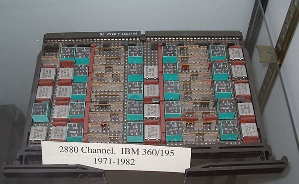
2880 Channel

2880 Channel
View in detail ⇗
© UKRI Science and Technology Facilities Council

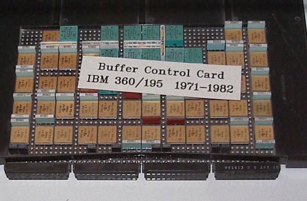
Buffer Control Card

Buffer Control Card
View in detail ⇗
© UKRI Science and Technology Facilities Council

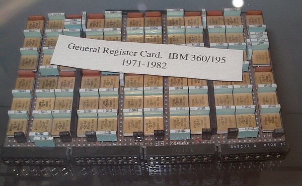
General Register Card

General Register Card
View in detail ⇗
© UKRI Science and Technology Facilities Council

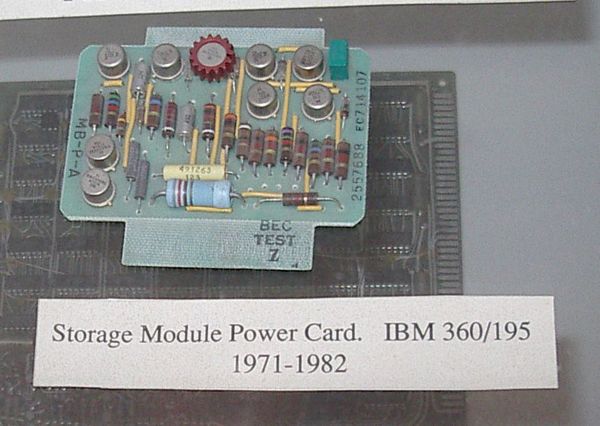
Storage Module Power Card

Storage Module Power Card
View in detail ⇗
© UKRI Science and Technology Facilities Council

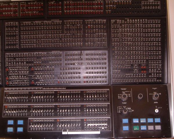
Close-up of 360/195 Console

Close-up of 360/195 Console
View in detail ⇗
© UKRI Science and Technology Facilities Council
⇑ Top of page
© Chilton Computing and UKRI Science and Technology Facilities Council webmaster@chilton-computing.org.uk
Our thanks to UKRI Science and Technology Facilities Council for hosting this site