
A simple block diagram of the ATLAS computer is given in fig. 1. The overall system is described elsewhere), and the main purpose of fig. 1 is to allow brief mention to be made of those parts of the computer which will not be discussed in detail in this paper.
A basic feature of the Atlas System is the extent to which complex operations are carried out by means of fixed store programs, e.g. a peripheral equipment requiring attention causes an entry to the appropriate fixed store routine. When necessary, the subsidiary core store is used as working space. Control operations such as start and stop are effected without having to extend the basic order code, by allocating special addresses to the various controlling flip-flops. Such addresses are termed V-store addresses, and it is principally by basic read-write orders to the several V-stores that the central unit exercises its control. V-store orders are also used to initiate transfers of blocks of information between the main core store and the magnetic tapes or drums. Once such a transfer has been initiated, intervention by the central control unit is not required; in fact the main program is continued, and an automatic priority circuit suitably interleaves word transfers between the main store and the drums, tapes, or central machine.
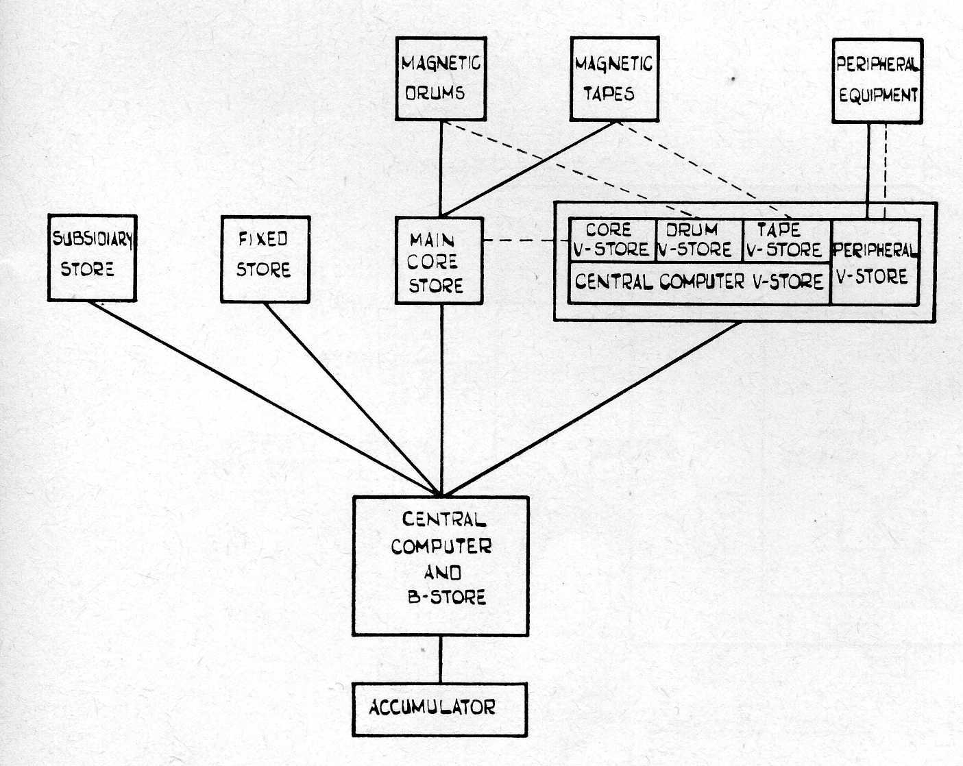
The remaining item in fig. 1 is the 48-bit floating point accumulator. The central control is not concerned in the detailed operation of the accumulator; its role is merely to call down operands as required.
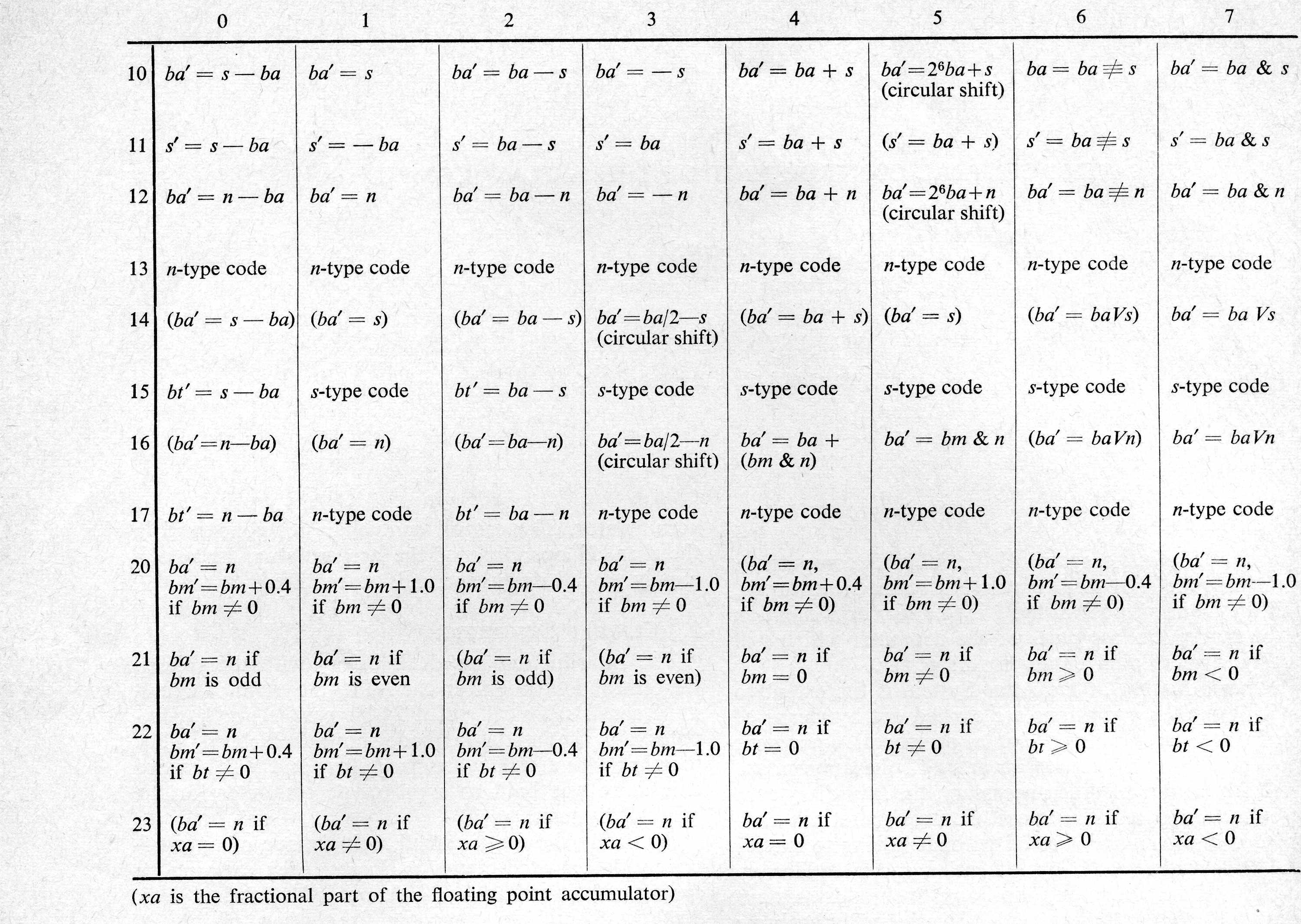
The Introduction has dealt briefly with the role of the central control unit in the ATLAS System. The unit itself consists basically of a 24-bit parallel mode computer with the instruction code shown in Table 1.
This, together with a 4000 word fixed store and a 1024 word core store was built as a prototype computer for the ATLAS System.
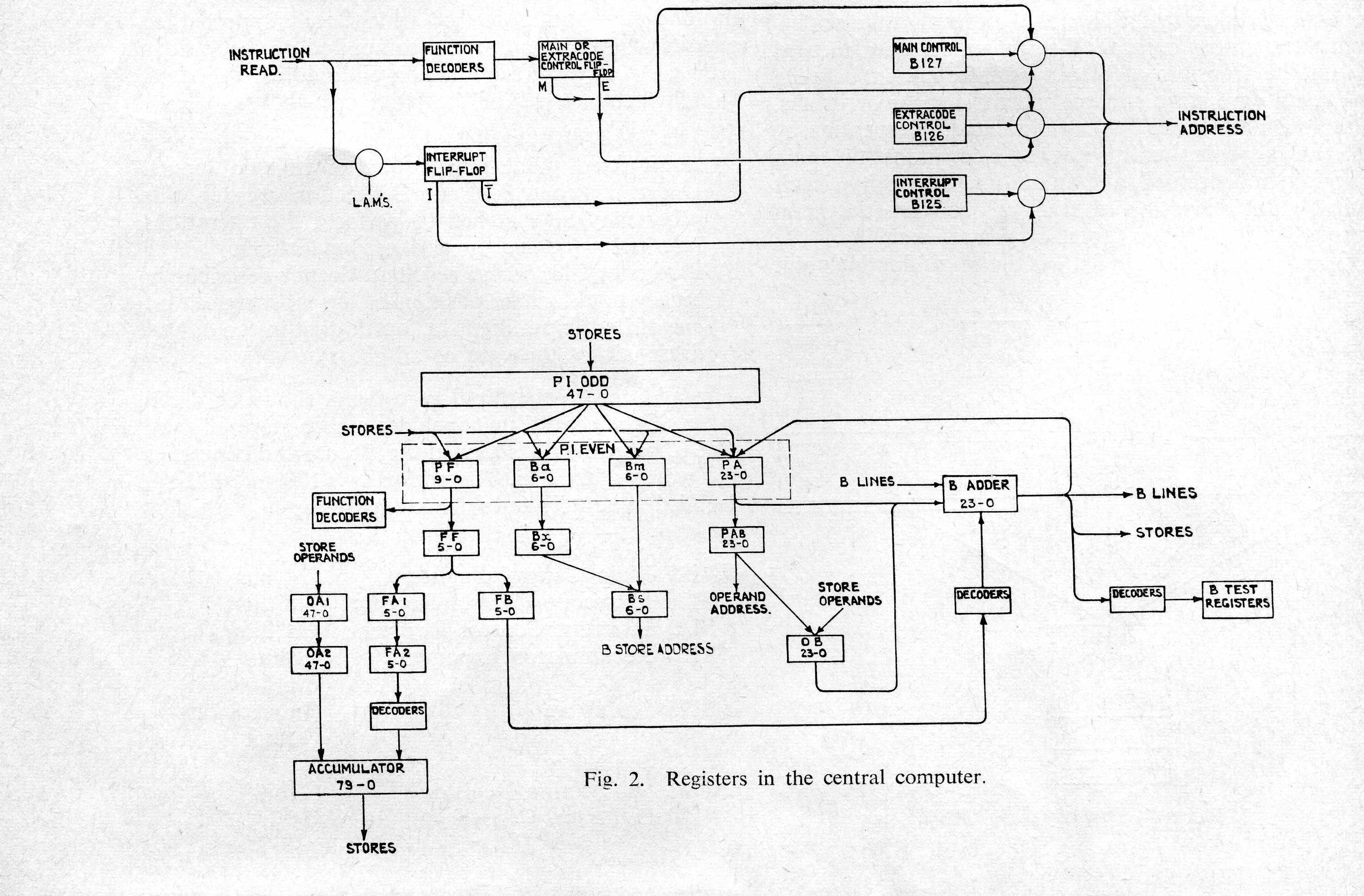
Physically the unit is small, being made of approximately 400 printed circuit packages (each carrying an average of 8 or 9 transistors), out of a total of over 5000 in the whole computer. It consists mainly of flip-flop registers, some of which are connected to circuits whose outputs are a compound of the various inputs. Apart from the function and address decoders, two important cases of the latter are:–
In addition to the flip-flop registers shown in detail in fig. 2, the central unit includes a core store of cycle time 0.7 µsecs. This is termed the B-store and comprises 120 words of 24 bits. The addresses B120 to B127 are decoded separately and refer to special flip-flop registers as follows:–
B127 Main Control Register      (24 bits)
B126 Extracode Control Register (24 bits)
B125 Interrupt Control Register (24 bits)
B124 Accumulator Exponent       (8 bits + 1 overflow bit)
B123 See above                  (Input 8 bits - Output 4 bits)
B122 See below
B121 Substitution Register      (7 bits)
B120 Lights on Console          (24 bits)
B register 122 has no physical existence; when B122 is named in the appropriate digits of an instruction, the seven bits contained in B121 are substituted and thus determine which line of the B-store is called down.
The instructions listed in Table 1, together with 64 Accumulator instructions constitute the basic instruction code of ATLAS. Extracode routines in the fixed store extend this basic repertoire. Some extracodes are fairly minor variants of the basic instructions, e.g. test bm > 0, whilst others are quite sophisticated subroutines, e.g. set the floating point accumulator to the arcsine of the specified operand. The precise division between the categories basic and extracode was decided after weighing the engineering factors of cost and complexity against the programming factors of time and space.
An order has the form
F(10 bits) Ba(7 bits) Bm(7 bits) S(24 bits)
For convenience of description, the function bits F are divided into a most significant binary digit F9 and 3 octal digits.
Bm usually denotes the address of a 24-bit word (or line) in the B-store, the contents of which are to be used to modify the 24-bit address part S of the instruction. In the case of test codes, Bm may specify the B register to be tested.
For orders involving the accumulator (A codes) the Ba digits are used in the same way as Bm to provide a second modification of the address.
For instructions not involving the accumulator (B or test codes), the Ba digits specify the B-store operand address.
After modification, the S digits may be used directly as an operand rather than as a store address. In instructions of this type it is customary to designate these digits by the symbol N.
It will be noted that control transfer or jump instructions are not provided as such; the more general order of the type Ba = N serves the same purpose if the appropriate B register (e.g., B127 if in Main Control) is named.
When an extracode instruction is detected by the presence of a 1 in F9, the normal address modification is carried out, but instead of proceeding directly with the operation at this point, the modified address is stored in B119 and Ba is stored in B121. Meanwhile, the flip-flop M/E is switched to the state E, thus ensuring that the next instruction from the store will be determined by the Extracode Control i.e. B126 (fig. 2). At the same time the function digits of the instruction are transferred to B126; these digits are arranged to refer to the appropriate entry point in the fixed store subroutine. The extracode routine may now refer to the required store operand through modification by B119, and to the required B register, in the case of B-type extracodes, by use of the substitute facility of B121 and B122.
Exit from the extracode routine merely requires the flip-flop M/E to be switched back to M after reading the final instruction. This is achieved without an explicit exit order, by duplicating the basic order code with F8 as a 1 instead of a 0 and using F8 as an extracode exit bit.
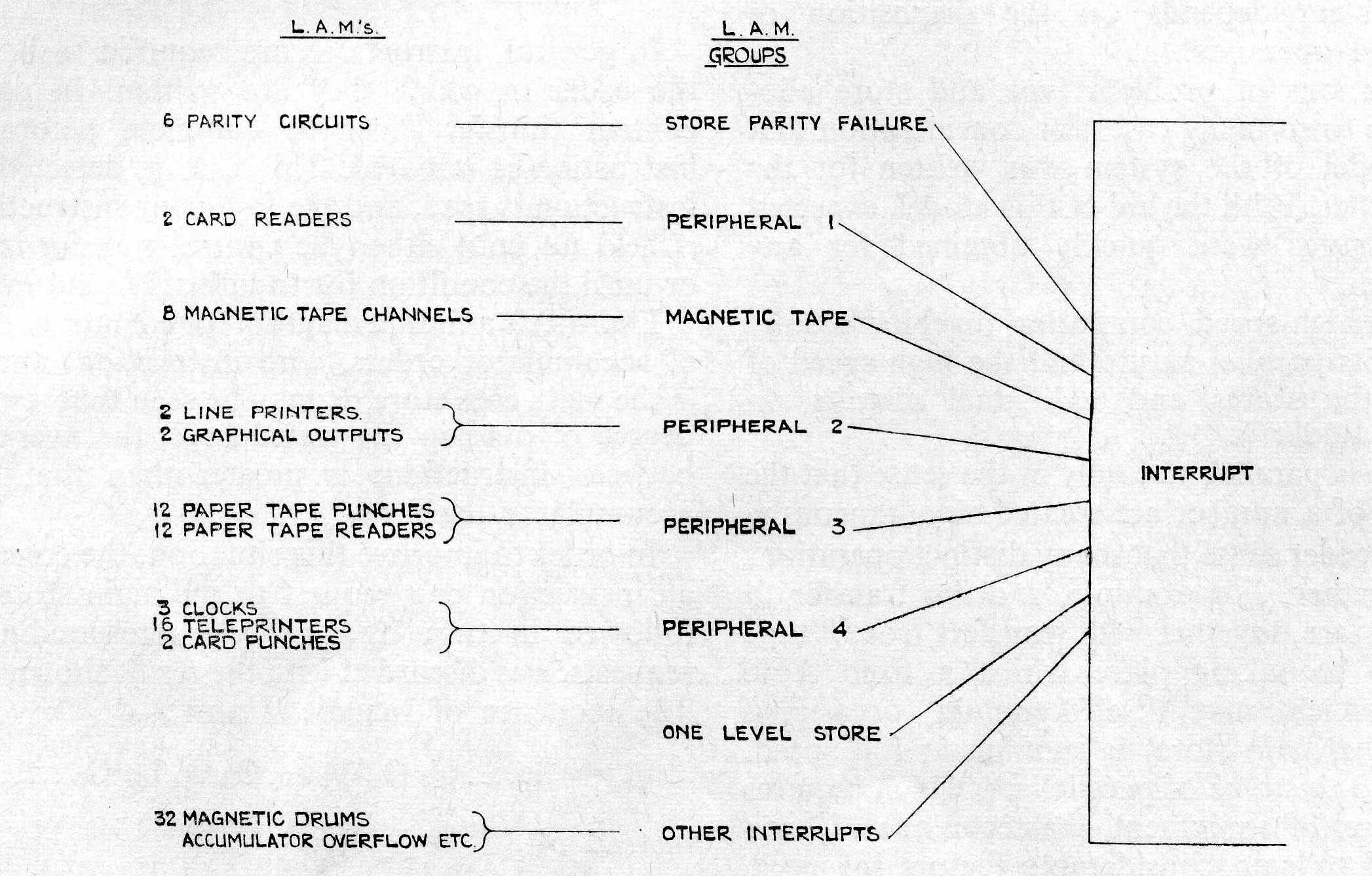
As may be seen from fig. 2, the waveform I determines that the Interrupt Control register B125 is the address source for an instruction request, regardless of the state of the M/E flip-flop. The cause of an interruption is termed an L.A.M. (look at me), and many of those shown in fig. 3 may occur at the same time. The OR of all possible L.A.M.s is examined each time an instruction is read. If any L.A.M. is present and control is not already set to Interrupt, I is set and the number corresponding to the general interrupt program entry point is inserted in B125. The first task of the interrupt program is to determine with appropriate priority which of the many L.A.M.s requires attention. To reduce the number of operations involved, the L.A.M.s have been grouped in order of priority and V-addresses have been assigned to groups, subgroups and individuals, the maximum number in any one address being 8. By successive reading of V-registers to B123, and modification by the output digits of B123, the source of interrupt of highest priority is located in five basic orders. From this point the appropriate routine is entered and the corresponding L.A.M. is reset to zero. When no further L.A.M.s are in the one state, control is returned to Main or Extracode by resetting the I flip-flop to not I.
The registers which constitute the central control unit are built with bistable transistor circuits which have a response time of approximately 50 nsec. Each entry to a flip-flop consists of a two input AND gate. One of these inputs is common to all digits of the register and is used for the transfer timing pulse or strobe. A nominal pulse width of 100 nsec is adopted throughout.
The problems involved in the logical design were:–
It is the detailed interpretation of item (3) which governs the decisions on items (1) and (2) and hence ultimately the form of the machine.
In order to estimate the overall computing speed for any proposed system it is necessary to examine a number of different types of program. This is complicated by the widely differing access times of the four types of store. Furthermore, the main core store is divided into several discrete access systems to overcome the limitations of cycle time. Thus the computation time of a particular problem depends on the disposition of instructions and operands.
The combinations of problem type and store allocation gave rise to so many cases for consideration that a program model of the system was written for the Mercury computer. With the aid of this model, expected performance figures were quickly obtained for any proposed design.
ATLAS is a high-speed computing machine mainly on account of its parallel nature and the high speed of operation of the stores and individual circuits, in particular, the adder.
The machine is parallel, not only in the sense that the individual bits of a number are treated simultaneously, but also in the wider sense that many distinct operations may occur together. For example, a drum transfer to the main core store, together with transfers from 8 tape channels, may be taking place whilst a fixed store programme (which may itself contain occasional references to the main store) is running at full speed.
In addition to this type of parallelism, which requires some duplication of equipment, the technique of overlapping is used to gain considerable factors in speed, with the minimum of additional hardware. Overlapping is made possible by dividing the sequence of operations of a complete instruction into several distinct stages.
This allows subsequent instructions to be initiated whilst earlier ones are still incomplete. In this manner, as many as six instructions may be in process at the same time, and in particular several short B-type instructions can be completed whilst an earlier long A-type instruction (e.g. division) is still in process.
The registers required for storing the necessary information for six instructions will now be described (cf. fig. 2).
Successive addresses in the main core store refer to different stacks, each with its own access equipment. The provision of two instruction registers, PIO and PIE, permits the reading of a pair of instructions in a single access time. Only single instructions are read from the fixed or subsidiary stores and they go into PIE.
For an accumulator instruction, the Ba and Bm digits are no longer required when modification is complete and the modified address digits PA are held in the appropriate store once the operand request has been accepted. After modification, only the 6 less significant function bits are needed to define the instruction, and these must be stored. In fact, two function registers FA1 and FA2, and two operand registers OA1 and OA2, are provided in the accumulator. These serve the dual purpose of ensuring the minimum gap between successive A-instructions, and allowing subsequent B-type instructions to proceed.
In the case of B-orders, the Ba digits are still required after address modification, and these are stored in Bx. The six less significant function bits are stored in FB and an operand register OB is provided for the 24-bit store operand or N.
Storage is thus provided for five functions by PFO, PFE, FA1, FA2 and FB. The sixth function storage register is FF which buffers transfers between PFE and FA1 or FB; the corresponding extra address register is PAB which acts as a buffer between PAE and the stores.
In general, instructions are required to be obeyed in the order in which they are written. In particular, a control transfer must be complete before the next instruction is initiated. This case is detected when the instruction is read, and the following instruction request is held up until either the control transfer is complete, or until the condition for transfer is found not to apply.
Fig. 4(a) is a timing diagram for a continuous sequence of accumulator orders, with instructions and operands in the main core store. It may be seen that, even with the degree of overlap illustrated here, the average interval between instructions is greater than that set by the accumulator itself.
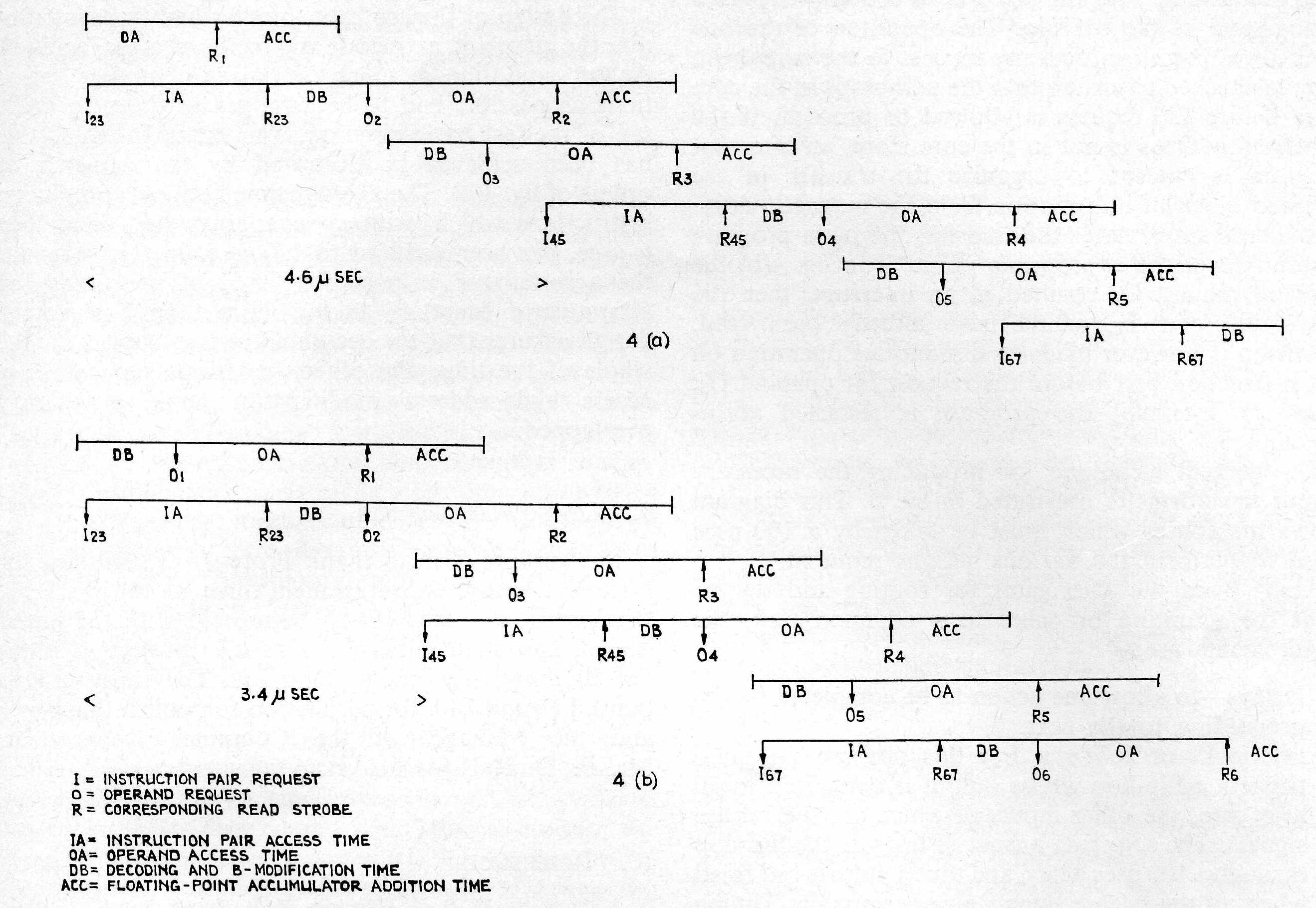
In order to improve this situation, the conception that an instruction pair request to the main store should be followed in turn by its two corresponding operand requests, was discarded with the result shown in fig. 4(b). The sequence of request is now:–
...I23O1O2I45O3O4I67O5...
instead of
...I23O2O3I45O4O5I67O6...
A switch from Main to Extracode or Interrupt Control does not generally require any special action with regard to the state of the overlap. The operation of the one level store requires that any request to the core/drum store is checked to ensure that the address is in the core store before the request is allowed to proceed. If the requested address is not in the core store, an interrupt program is entered to organize the transfer of the required block of information from the magnetic drum to the core store. After the transfer, the main program is restarted at the appropriate point. If in fig. 4(b) the operand request O3 resulted in an interrupt, then the instruction pair I45 would have already been read. Provision is however made to discontinue operation on this instruction pair before the request for operand O4. After the interrupt the program is restarted at instruction 3.
The general technique for producing the necessary timing waveforms is illustrated in fig. 5. This diagram shows the routes which must be taken by a 100 nsec pulse to perform the various actions required.
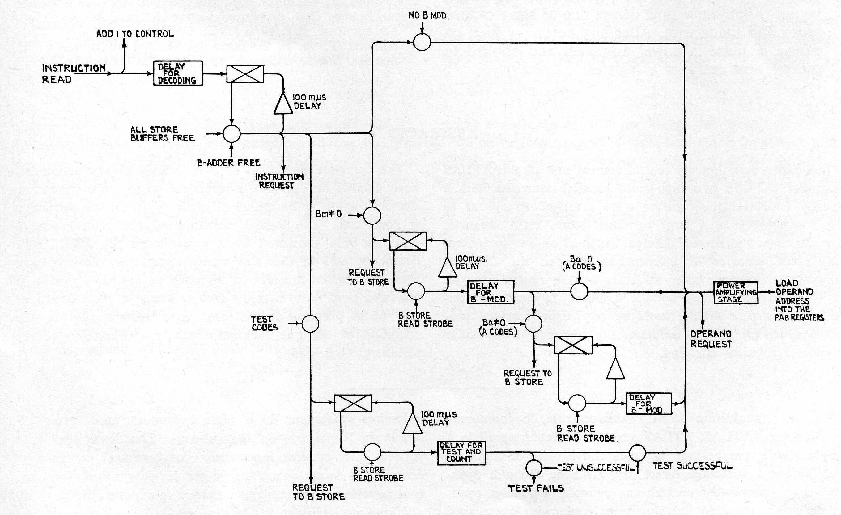
Apart from the AND gates for routing and the OR gates for reuniting branches to a common task, the requirements are:–
The design of the central computer had to accommodate the interrupt, extracode and one-level store facilities. At the same time, as much overlap of computer operations as possible had to be arranged in order to make use of the fast basic circuitry. The extent to which this has been achieved is illustrated by the sequence of orders of fig. 4(b). The average time between completing instructions which, with no overlap, would have been 6 µsec, has been reduced to 1.7 µsec. In this sequence the accumulator is busy for 70% of the time. For accumulator functions taking more than 2 µsec, the design ensures that the accumulator is occupied for the whole of the time, the other operations such as store access and address modification being completely overlapped.
The authors wish to thank Professor T. Kilburn for his direction and encouragement throughout, Mr. E. T. Warburton who was closely connected with the initial design, and all members of the Atlas project at Manchester University and Ferranti Ltd. They also wish to thank Ferranti Ltd. for permission to publish this paper and the Manager of the Computer Department, Mr. P. D. Hall for his encouragement.
(1) Kilburn, T., D.B.G. Edwards, R.B. Payne, and E.T. Warburton: ATLAS (To be published).
(2) Kilburn, T and R. L. Grimsdale: A Digital Computer Store with a Very Short Read Time. Proc. IEE 107B (1960) 567.
(3) Kilburn, T., D.B.G. Edwards and D. Aspinall: A Parallel Arithmetic Unit Using a Saturated-Transistor Fast-Carry Circuit. Proc. IEE 107B (1960) 573.
(4) Kilburn, T., D.B.G. Edwards, M.J. Lanigan and F.H. Sumner: One Level Storage. IRE Trans. EC-11 (1962) 223-235.
The paper describes the central control unit of the ATLAS computer. ATLAS is a high-speed parallel computer with a directly addressable core/drum store arranged to appear to the programmer as a large one-level store, eight magnetic tape channels and several different types of on-line peripheral equipment. Transfer of information between the different stores is autonomous after initiation by the central control. All the peripherals may operate together, as they are controlled on a time-sharing basis by permanently stored programs which are entered automatically whenever a particular peripheral requires attention.
The complete operation of each individual instruction has been divided into several independent stages, thus permitting one instruction to be initiated before the previous instruction is completed. The logical structure of the central control unit has been simulated by a program on the MERCURY computer, and in this way many engineering designs have been investigated in order to approach an optimum system. It has been possible to arrange that as many as six instructions may be in progress at the same time without affecting the operation of the one-level store, the magnetic tapes or the peripheral equipments.
