
This note describes a special feedback technique leading to the design of a D.C. coupled trigger circuit which has more than two states of stable equilibrium, and which may be triggered from a quiescent or central state to any of the other states by an appropriate input signal and subsequently reset to the quiescent state by a special resetting signal. To illustrate the practical application of this technique, an example is given of a circuit designed to form the basic element of the registers or staticizers of a three state parallel operated digital computer embodying the principles of checking outlined in section (5.2) of the conference note by Dr. A.M. Uttley entitled Checking Procedure and Circuits.
The fundamental triggering mechanism used is essentially that of the well known Eccles-Jordan circuit, which consists basically of two phase inverting amplifiers in cascade with the output terminals of the second amplifier back-coupled to the input terminals of the first, so that a positive feedback loop of high gain is produced, giving rise to a state of unstable equilibrium with both amplifiers in the middle of their respective characteristics and to two states of stable equilibrium symmetrically disposed with respect to the central or unstable state. The central state of such a circuit may be made stable, however, if the back-coupling network between the amplifiers is of such a type as to provide zero transmission when the amplifiers are in the middle of their characteristics. This can be accomplished by using two positive feedback networks and inserting in series with each network a diode biassed so that neither network conducts when the circuit is in its central state but so that either one or the other conducts when the output level from the second amplified is displaced somewhat from the central position. Such a trigger circuit will have three states of stable equilibrium.
Feedback networks of the type referred to may be termed conditional feedback networks. When the circuit is displaced from its central state and one or other of the conditional positive feedback networks thereby brought into operation, the total excursion of the amplifier output points may be limited before either amplifier runs off its characteristic by arranging that one or other of two conditional negative feedback networks around one of the amplifiers comes into operation and reduces the differential gain around the overall positive feedback loop to below unity.
Two further states of stable equilibrium may be obtained if a further pair of conditional positive feedback networks is provided such that one or other comes into operation if the output level from the second amplifier is displaced beyond the value corresponding to one of the first non-central states of stable equilibrium, thus restoring the gain around the positive feedback loop to a value greater than unity. This process of providing conditional positive and negative feedback networks arranged to override one another in turn as the output level from the second amplifier is more and more displaced from its central value may, in theory at least, be continued until one of the amplifiers overloads so that there is no clearly defined limit to the number of states of stable equilibrium obtainable.
Obviously many different practical arrangements are possible for the amplifiers and their associated feedback paths, but for elegance and ease of analysis, a highly convenient arrangement is one in which the first amplifier is of the anode follower type, the various feedback networks and the source of input signals being arranged to supply currents into the virtual earth existing at the grid of this amplifier. The second amplifier may conveniently take the form of a unity gain phase inverter, and may also he of the anode follower type.
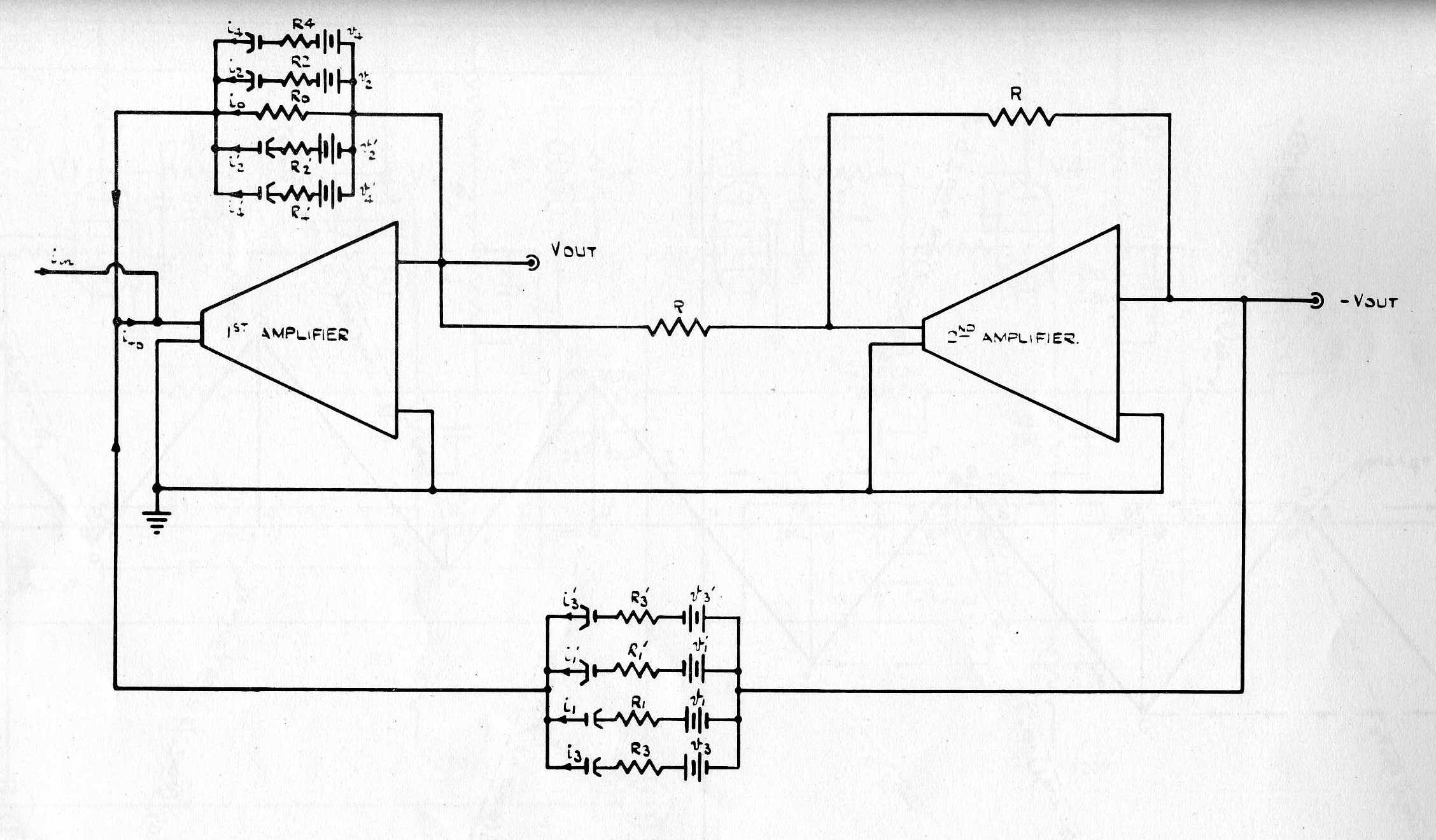
Fig.1 shows a schematic of a circuit arranged to have five states of stable equilibrium. Each amplifier is presumed to have very high internal gain and to be phase inverting. A feedback resistance R0 is connected between the output and input terminals of the first amplifier. The second amplifier is arranged with equal input and feedback arms of value R, and may hence be regarded simply as a unity gain phase inverter of the output voltage vout from the first amplifier. The resistances R1, R3, R1 and R3 each in series with a diode and battery are the conditional positive feedback paths, whilst resistances R2, R4, R21 and R41 each in series with a diode and battery are the conditional negative feedback paths. When vout is zero, -vout is also zero and all the conditional feedback paths are of zero conductance. This represents the central or quiescent state of the circuit. Now let v41 < v31 < v21 < v11 < 0 < v1 < v2 < v3 < v4. Also put 1/Rn = Gn. The total feedback current ifb to the input terminal of the first amplifier may now be considered as a function of vout. We have:-
ifb = i0                     = G0vout ... ...                                                     [0  < vout < v1]
ifb = i0 + i1                = G0vout - G1(vout-v1)      ...                                      [v1 < vout < v2]
ifb = i0 + i1 + i2 + i3 + i4 = G0vout - G1(vout-v1) + G2(vout-v2)                           ...   [v2 < vout < v3]
ifb = i0 + i1 + i2 + i3 + i4 = G0vout - G1(vout-v1) + G2(vout-v2) +G3(vout-v3)              ...   [v3 < vout < v4]
ifb = i0 + i1 + i2 + i3 + i4 = G0vout - G1(vout-v1) + G2(vout-v2) +G3(vout-v3) +G4(vout-v4) ...   [v4 < vout]
A similar set of equations is obtainable for negative values of vout. If the first amplifier be presumed free from grid current, the current ifb must be balanced by an equal and opposite current from an input source, and we can therefore write -iin = ifb.
In fig.2, ifb is plotted against vout. The dotted lines OS, O1T, O2U, O3V and O4W represent the equations for i0, i1, i2, i3, and i4 respectively, and the ordinates of the curve OABCDE representing the equation for ifb are obtained by adding the corresponding ordinates of the above five lines. The curve OA1 B1 C1 D1 E1 corresponding to negative values of vout is similarly derived. The conditions that the slopes of the portions AB and CD, corresponding to the regimes [v1 < vout < v2] and [v3 < vout < v4] respectively, shall be negative are that G1>G0 and G1 + G3 > G0 + G2. Similarly, the conditions that the slopes, of the portions BC and DE, corresponding to the regimes [v2 < vout < v3] and [v4 < vout] respectively, shall be positive are that g1 < G0+G2 and G1+G3 <G0+G2+G4. In Fig.2, all these conditions are assumed fulfilled and it is further assumed that the values of v1, v2, v3, v4 are chosen so that the curve OABCDE crosses the vout axis once during each regime and so that the value of ifb corresponding to v0ut = V3 (point C) is higher than that corresponding to vout = v1. The corresponding conditions for negative values of vout are also assumed fulfilled. Then the segments E1D1, C1B1, A1A, BC and DE represent regimes of stable equilibrium and the segments D1C1, B1A1, AB and CD), of unstable equilibrium. The points Q1, P1, O, P and Q represent the five states of stable equilibrium corresponding to zero values of ifb or iin. If, starting from the central position 0, -iin is steadily increased, the operating point moves along OA and as soon as -iin exceeds Gov1 (point A) a sudden transition to point F on BC occurs, and in this case, as -iin is decreased to zero, the operating point moves back along ED to Q. The points P1 and Q1 may be reached in a similar manner by supplying negative values of -iin to the circuit.
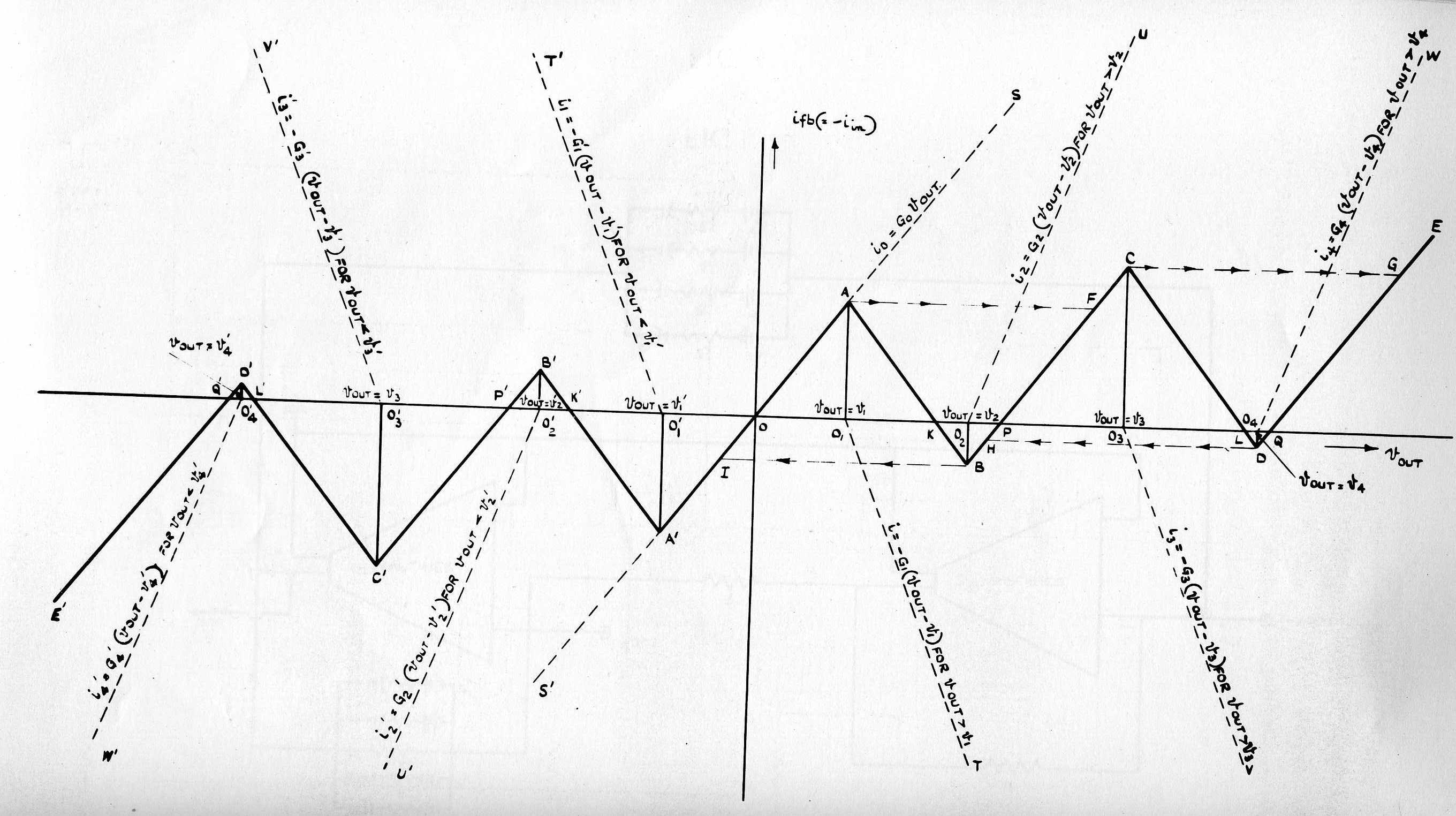
It is to be noted that if, whilst iin is zero, all the conditional positive feedback paths be momentarily open-circuited, vout will immediately become zero. By this means the circuit may be reset to its central state from any non-central state.
Finally, it is of interest to note that if G41 = G31 = G21 = G11 = 2G0 = G1 = G2 = G3 = G4, then in the stable regimes d ifh/d vout = G0, whilst in the non-stable regimes d ifh/d vout = -G0, and hence the slopes of all the segments of curve E1D1C1B1A1ABCDE are of equal numerical value.
Fig.3 shows the essentials of a design found satisfactory for the purpose mentioned in the Introduction.
The first amplifier comprises a high gain pentode V1 and a cathode follower V2 the negative feedback paths being supplied from V2 cathode. The cathode follower is included to provide a tough output point. The second amplifier is of similar design around V3 and V4. R1 puts negative feedback on the first amplifier under all conditions. R6C3 and R7C4 are the input feedback arms of the second amplifier and are made equal so that this amplifier functions as a phase inverter of unity gain. The conditional positive feedback paths to V1 grid are provided by R12 in series with D1 and R13 in series with D2, the resistances R12 and R13 being supplied from points arranged to be about five volts negative and five volts positive respectively in relation to V2 cathode so that in the quiescent state of the circuit these feedback paths are open circuited. The conditional negative feedback paths comprise diodes D3 and D4 fed from points thirty volts negative and thirty volts positive respectively in relation to V2 cathode. In order that the outputs at the cathodes of V2 and V4 shall be as accurately as possible limited to thirty volts peak when the circuit is in an active state, no resistances are included in series with D3 and D4. The output points X and Y are connected to the cathode followers through small LR networks in order to avoid capacitative loading of the cathode followers at high frequencies, this being liable to lead to the generation of high frequency oscillations. The small condensers C1 and C2 are for the purpose of stabilising the feedback amplifiers.
Now when the circuit is used as an element of a register in a digital computer, it will normally be required, on the receipt of a gating pulse, to take up the configuration of some corresponding trigger circuit in another register. V5 and V6 are gating valves, their cathodes being connected to the output points Y1 and X1 of some similar trigger circuit. The grids of V5 and V6 are normally held at fifty volts negative to earth but are brought up to earth by the gating signal, whereupon a negative current will be supplied to the input of either V1 or V3 according to whether Y1 or X1 is negative. X and Y will then assume the same polarities as X1 and Y1 respectively. As virtual earths exist at the input grids of V1 and V3, several gating valves may be joined to these points without interaction. The circuit is reset to its quiescent state from an active state by open-circuiting whichever of the positive feedback paths is in operation. This is accomplished by small negative and positive pulses applied to the cathode of D5 and anode of D6 respectively.
